
HBM Memory

The Dual Impact of HBM Reliability Test Standard Upgrades on Yield and Cost
High Bandwidth Memory (HBM) has moved into the mainstream of advanced computing, powering AI accelerators, high‑end GPUs, and cutting‑edge server platforms. As deployment scales and workloads become more demanding, the industry has steadily tightened reliability expectations for HBM devices. This has led to upgraded reliability test standards across thermal, electrical, mechanical, and system‑level dimensions.

HBM4 Mass Production Kickoff: The 2026 Tech Roadmap Showdown Among 3 Memory Giants
By 2026, high bandwidth memory (HBM) has moved from a niche enabler of premium accelerators to a central battleground in the AI and advanced computing industry. The kickoff of HBM4 mass production marks a decisive escalation: the three leading memory giants are no longer just supplying components; they are effectively shaping the performance envelope and cost structure of the next generation of AI chips.

Interpreting the Capital Market Signals of Samsung’s HBM3E Nvidia Certification
Samsung’s public announcement that its HBM3E modules achieved Nvidia certification is more than a product milestone—it sends multi-layered signals to capital markets about demand, competitive positioning, supply-chain dynamics, and future cash flows across memory makers, OSATs, accelerator OEMs, and equipment vendors.
TSV Technology Iteration in HBM – New Requirements for Equipment Suppliers
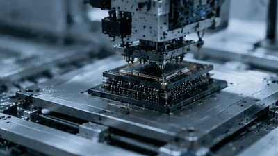
Through successive HBM generations the through-silicon via (TSV) has evolved from a tactical enabling feature into a strategic differentiator. As HBM moves from HBM2E and HBM3 to HBM3e and HBM4, TSVs must support finer pitches, lower parasitics, higher thermal conduction needs, and coexistence with hybrid-bond planes. These requirements cascade into new expectations for equipment suppliers across lithography, etch, deposition, CMP, inspection, and metrology.
Incremental Demand for HBM Test and Burn-in Equipment – A Quantified Forecast
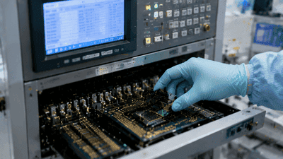
As High-Bandwidth Memory (HBM) moves from niche to mainstream across AI, HPC, and advanced graphics, test and burn-in equipment emerges as a critical bottleneck. HBM modules require more extensive, higher-fidelity testing than commodity DRAM: multi-die functional tests, high-speed channel validation, thermal stress profiles, and system-level burn-in under representative accelerator loads.

Hybrid Bonding Adoption in HBM4 and Its Supply Chain Opportunities
Hybrid bonding—a suite of direct copper-to-copper and copper-to-dielectric bonding techniques—has become central to the HBM4 roadmap. Where previous HBM generations relied primarily on micro-bumps and through-silicon vias (TSVs), HBM4 pushes signaling density and electrical performance to levels that make hybrid bonding not optional but essential.

Global HBM Patent Landscape Competition: The US-China-Japan-Korea Power Game
High-Bandwidth Memory (HBM) has become one of the most strategically important technologies in the AI and high‑performance computing era. Patents around HBM architectures, hybrid bonding, TSVs, interposers, thermal solutions and test methods now form a dense web of intellectual property that shapes who can manufacture, license and profit from AI memory at scale. The global HBM patent landscape is increasingly a power game among the United States, China and Japan, layered on top of Korean and Taiwanese industrial strengths.

HBM’s Value Share Per AI Server Unit Continues to Rise
High-Bandwidth Memory (HBM) has steadily transitioned from a niche premium to a core system-level enabler for modern AI servers. As models grow larger and throughput demands intensify, designers increasingly attach value to bandwidth, density, and energy efficiency that HBM uniquely provides.

Breakthroughs in Wafer Warpage Control During HBM Manufacturing
Wafer warpage has long been a critical yield and reliability concern in advanced semiconductor packaging, and it is especially consequential for High Bandwidth Memory (HBM). HBM’s stacked-die architecture, use of through-silicon vias (TSVs), and reliance on precise bonding and micro-bump formation all amplify the impact of any deviation from flatness. Recent breakthroughs in warpage control—spanning materials science, process engineering, metrology, and modeling—are improving yields, reducing costs, and enabling larger HBM stacks with higher interconnect densities.
Big 3 Memory Makers’ HBM CapEx Share Exceeds 50% for the First Time in 2026
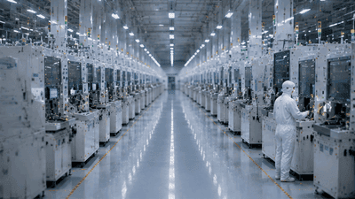
In 2026 the semiconductor landscape reached a decisive inflection: the combined capital expenditure (capex) directed by the industry’s Big Three memory makers—SK Hynix, Samsung, and Micron—toward High-Bandwidth Memory (HBM) and its enabling packaging technologies exceeded 50% of total industry HBM-capex for the first time. This milestone matters because it signals concentrated investment toward premium memory and packaging ecosystems that underpin AI accelerators, HPC clusters, and advanced datacenter architectures.
Popular

Narrowing Spread Between NAND Spot and Contract Prices in 2026 – A Signal
By 2026, one of the most watched metrics in the NAND flash market has started to shift in a subtle but meaningful way: the spread between spot prices and long‑term contract prices is narrowing. For casual observers, this may look like just another incremental change in a notoriously volatile industry. For memory makers, module houses, device OEMs, and data center buyers, however, a tightening gap between spot and contract prices is a signal—a reflection of evolving supply–demand balance, risk perceptions, and strategic behavior on both sides of the market.

Price Divergence Trading Strategies Between NAND Flash and DRAM ETFs
NAND flash and DRAM sit at the core of AI storage and computing power. Both are memory, but they are not the same business. DRAM is main memory—fast, volatile, and central to high‑bandwidth workloads like AI training and inference. NAND is non‑volatile storage—slower than DRAM, but crucial to persistent data and large‑scale object storage. The cycles that drive their pricing and margins overlap, yet they often diverge. That divergence is where trading strategies between NAND and DRAM ETFs become interesting.

China’s HBM Localization Progress: The Catch-Up Pace of CXMT and XMC
China’s drive to localize advanced memory technologies has accelerated over the past several years. High-Bandwidth Memory (HBM) sits near the center of that strategy because it is integral to AI accelerators, high-performance computing (HPC) and other strategic compute platforms. Two domestic players—ChangXin Memory Technologies (CXMT) and XMC (Xianghui Memory, commonly referred to as XMC)—have become focal points in assessing how quickly China can close the gap with international incumbents on HBM die, stacking, and packaging.